
There is a fundamental disconnect between the cadence that chip makers want for their devices and what the hyperscalers and cloud builders would prefer. And it looks like they are working together to split the difference and accept a two year cadence for the architectural upgrade cycle for all key compute and networking functions. And that is cadence going to apply to everything from CPUs to GPUs to FPGAs to DPUs and SmartNICs.
If left to their own devices – or rather those etched and packaged for them by their suppliers – the hyperscalers and cloud builders would want more powerful and less costly devices each year, with the consequent improvement in price/performance for compute and networking each time they replace a third or a quarter of their equipment fleets, which they do every year. An annual cadence for big architectural changes in any specific product line is difficult, and so is playing the tick–tock manufacturing method made famous by Intel, where a chip process improvement happened on an old architecture and was followed they next year by a new and improved architecture for that device. Moore’s Law leaps in performance and reductions in chip costs happen over longer time spans now – process nodes are more like three years apart these days – so this is all tough to make run in phase. And so, a two year cadence splits a lot of differences, and that is why roadmaps all over the IT sector for datacenter products are marching to that step.
The interesting thing we will observe is that IT chip makers are trying to change only some chips each year and do their launches out of phase so they have something new to talk about and to sell each year. Eventually, we think shipments of CPUs, DPUs, and switch ASICs, and network interface cards will line up, whether the vendors like it or not, because hyperscalers and cloud builders want all new stuff in their new systems. Ditto for enterprises. Intel server CPU roadmaps haven driven network switch purchases for about two decades now, for instance.
So, in the end, the early and volume shipping of products will probably all line up even if the announcements of devices do not.
Offload, Or Be Offloaded
In the wake of the Great Recession, Intel had hegemony in datacenter compute, and not much in the way for CPU competition and huge margins driven by flattening price/performance improvements and very high operating income for its Data Center Group. We have shown this curve time and again. (Here in 2017 and then there in 2021, for instance, with Xeon and Xeon SP processors.) But those profits and Intel’s inability to get process improvements to drive increasing core counts on its Xeon SPs meant that every core became a precious and expensive commodity, and therefore everyone started looking around for where to offload some of the work that was pulled onto the CPU and its hypervisor and operating system.
And thus, SmartNICs were born and evolved into what most people are calling Data Processing Units, or DPUs, but which Intel is calling Infrastructure Processing Units, or IPUs. We concede that data processing is mostly done on CPUs and that what DPUs are mostly doing they are being architected today is handling the virtualization of the system (running the hypervisor) and the network or access to it (through virtual switches and interfaces) and providing security and other services that in some fashion move work off the CPUs inside of a server. In a way, all of the virtualized functions that were added to operating systems and drivers are being consolidated on a dedicated and cheaper subsystem – just like mainframes and proprietary minicomputers did five and four decades ago because mainframe CPUs were also very expensive commodities.
Intel may have been a little late to the DPU party, but it is making up for lost time through a partnership with Google for its “Mount Evans” DPU, which we got a preview of last August.
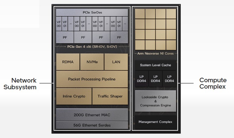
As you can see from the block diagram above, the Mount Evans device has a network subsystem and a compute complex on the same device. (We are not going to presume it is one piece of silicon, but it could be.) On the network subsystem, there sixteen lanes of PCI-Express running at 4.0 speeds on SerDes, and four 56 Gb/sec SerDes for Ethernet I/O that, after encoding, deliver 200 Gb/sec of connectivity out of the device. The PCI-Express links the DPU to the CPU in the system, and the Ethernet MAC with RoCE v2 support links the DPU to the network; a programmable packet processing engine, which we strongly believe was taken out of the heart of the “Tofino” family of switches that Intel got when it acquired Barefoot Networks a few years ago, allows for the P4 programming language to be used to manipulate data before it reaches the CPU and after it comes out of the CPU at line rate, and presumably also does the same for the on-package compute complex in the Mount Evans device. That compute complex has sixteen Neoverse N1 cores licensed from Arm Holdings plus various levels of CPU cache and LPDDR4 memory that is commonly used in laptops, plus accelerators for data compression and cryptography.
Now, Intel is committing to not only commercializing the Mount Evans device it co-developed with Google, but is committing to a roadmap for its hybrid FPGA-CPU DPUs as well. (It is interesting that the FPGA-only SmartNICs such as the “Arrow Creek” one announced last summer, are not part of the roadmap shown below, and that implies that they are not DPUs because they don’t have their own dedicated CPU compute.) Here is what the plan looks like:
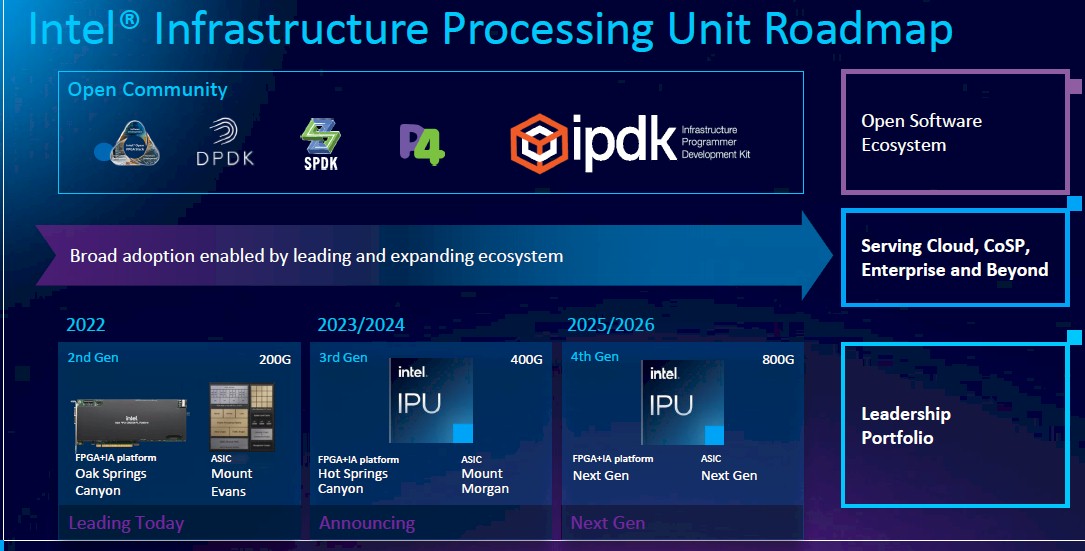
The “Oak Springs Canyon” DPU, which was revealed last summer as well, pairs and Agilex FPGA and a Xeon D processor together with 16 GB of DDR4 memory and two 100 Gb/sec Ethernet ports to accelerate certain network functions, notably data encryption but also including acceleration by the running of Open vSwitch virtual switching for hypervisors and NVM-Express over Fabrics and RoCE RDMA protocols on the device.
Both Mount Evans and Oak Springs Canyon are shipping to hyperscalers and cloud builders this year.
Looking out to 2023 and 2024, Intel’s plan is to deliver kickers to these DPUs, called “Mount Morgan” and “Hot Springs Canyon” respectively, and it is not clear which will come first and when – that is a pretty wide launch window. Both of these DPUs will have support for 400 Gb/sec Ethernet interfaces. Two years later, Intel is promising to deliver custom ASIC and FPGA accelerated DPUs with 800 Gb/sec Ethernet interfaces, and again, there is not a lot of precision here. You can guess the FPGA versions come out in 2023 and 2025 and the custom ASIC ones come out in 2024 and 2026, but there is no data to support such guessing. For all we know, Intel is hedging on the timing for both DPU families, not one.
What we can say is this: 2022 is a big CPU year and Intel needs to get both Oak Springs Canyon and Mount Evans devices out concurrent with “Sapphire Rapids” Xeon SP processors later this year. On Intel’s CPU roadmap and the more detailed one we made up ahead of Intel’s roadmap reveal in February out of frustration, 2024 is a big year for CPUs, with Intel delivering its “Granite Rapids’ Xeon SP. And it is reasonable to expect that 2026 is also going to be a big year for Intel Xeon SP CPUs, too. And thus we expect the N+2 generation of Intel DPUs (third gen for the custom ASIC variant and fourth gen for the FPGA accelerated one) to hit the market in volume 2026, no matter when it is actually announced. And if the DPUs come out ahead of the CPUs, no big deal – they will work in prior CPUs. But if the major CPUs come out late – Sapphire Rapids, Granite Rapids, and whatever comes after Diamond Rapids (due in 2025) in 2026 – they will stall volume purchases of the DPUs.

oneAPI 2023: One Plug-In To Run Them All
Intel has a lot at stake with its oneAPI software stack. A cross-platform parallel programming model, oneAPI is designed to fit into a highly diverse, heterogeneous – and increasingly cloud-based – infrastructure environment by enabling developers to stretch a single code base over multiple and varied architectures. In a world …
The Future Is Still Wide Open For Arm In The Datacenter
There is no question that that the combination of Nvidia and Arm Holdings would have been a powerful one in the datacenter. This is something that we have discussed at length before Nvidia launched its $40 billion acquisition of Arm Holdings, when Nvidia actually launched the takeover a year and …
Who Will Build Europe’s First Exascale Supercomputer – And With What, And Why?
Exascale supercomputing is just as important to Europe as it is to the United States and China, but each of these geopolitical regions on Earth has its own way of developing architectures, funding their development and production, and figuring out where the best HPC centers are to host such machines …
Be the first to comment