This article is more than 1 year old
Micron stacks its 3D NAND high in 2015
Technology continuing to scale with ‘higher densities, lower cost per bit’
Intel recently made a splash about its 3D NAND intentions. Knowing that Intel basically works with Micron on flash through the joint IMFT business, we asked Micron NAND marketing head Kevin Kilbuck about Micron's 3D NAND activities.
El Reg: Why is 3D NAND needed?
Kevin Kilbuck: Micron has been working on 3D NAND technology for more than five years as a solution for continued NAND scaling. In order to continue driving greater adoption of flash storage, NAND must continue to scale with higher densities and lower cost per bit.
However, creating a planar NAND cell smaller than 15nm isn’t likely to be competitive commercially, so planar NAND is essentially as dense as it will get. 3D NAND - stacking arrays of cells vertically within each die - is the logical progression to overcome these scaling limitations and continue to increase the capacity on each die.
El Reg: What is the overall structure of a 3D NAND chip?
Kevin Kilbuck: The basic architecture takes a planar (2D) array of cells and stacks multiple levels of them. It’s roughly analogous to taking a single-story building design and distributing the rooms into a 32-story tower instead. In 2D design, we kept shrinking the size of the rooms in the building (34nm, 25nm, 20nm, 16nm) so we could get more capacity without increasing the footprint.
Now that we’re gaining the majority of the capacity from the vertical dimension the design node isn’t so critical, so we can make the “rooms” bigger, so relaxing some of the design constraints we had begun to run into during 2D design.
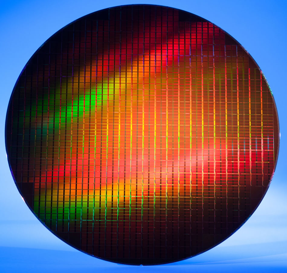
Micron 16nm NAND wafer
El Reg: How does a 3D NAND chip compare and contrast with a current MLC 2D Planar NAND chip in terms of capacity, IOPS, and sequential bandwidth and endurance?
Kevin Kilbuck: Capacities with Micron’s 3D NAND will double from where we are today. We’ll reach 256GB with our 3D NAND parts. While IOPS are system-dependent, bandwidth will see a significant boost at the die level. New features will help reduce latencies in most systems.
We also expect endurance to go up, due to the fact that we’re able to relax the size of the NAND cells (because the capacity we need is delivered primarily by the number of levels, not the size of the cells, as was true with 2D).
El Reg: How will 3D NAND chips scale in terms of capacity and what cell geometries are likely to be used?
Kevin Kilbuck: Our first 3D NAND parts will be 256GB for MLC and 384GB for TLC. We plan to relax the cell geometries to provide headroom for future scaling. We aren’t revealing the dimensions of the cell at this point, but I can tell you it will be larger than 20nm.
As I described above in the building analogy, the number of layers in the 3D stack is really a more important than the process node once you make the leap to 3D.
El Reg: For which markets does Micron see 3D NAND being suitable?
Kevin Kilbuck: 3D NAND should suit all the markets flash currently serves, but it’s likely that the increased cost efficiency and capacity that 3D NAND offers will open up new markets as well. What those markets are remains to be seen, but we’re already having conversations with customers who are very excited about the possibilities.
El Reg: In what form factors will 3D NAND appear (FlashDIMM, PCIe card, M2, SSD, etc)?
Kevin Kilbuck: 3D NAND will not increase the package size from our 16nm planar NAND, so it will appear in the same sorts of packages we’re currently shipping.
It may be important to clarify here that despite the towering descriptions above, the stacking is occurring at an extraordinarily small and precise scale; 3D NAND die won’t be noticeably taller than 2D NAND die. And like 2D NAND, we’ll stack multiple 3D die in a NAND package to achieve greater capacities in the single chip packages that you see in end products.
El Reg: Will TLC 3D NAND appear? What cell geometry, performance and endurance might be expected?
Kevin Kilbuck: Yes. Performance and endurance will be greater than what TLC is currently able to provide in planar designs.
El Reg: Will SLC 3D NAND appear? What cell geometry, performance and endurance might be expected?
Kevin Kilbuck: Micron is not planning to provide SLC parts in 3D NAND. We expect the 20nm SLC parts we currently offer will meet the market demands for purpose-built SLC Flash for the foreseeable future.
El Reg: When will 3D NAND products appear and how will existing 2D NAND products transition to 3D NAND products?
Kevin Kilbuck: Micron will be sampling MLC 3D NAND parts in the spring of 2015; TLC will follow shortly thereafter.
The transition from 2D to 3D will happen first on applications that are driving larger capacities, such as like SSDs. We expect all of the high-volume flash markets to transition to 3D NAND over time.
PLEASE NOTE: We also asked Toshiba, SanDisk's flash partner, similar questions about its 3D NAND intentions and received a polite brush-off from a spokesperson, who said “unfortunately, Toshiba is unable to provide information regarding your specific questions, but we’ll be sure to keep in touch and we’ll circle with you when we have more information that we can share".
We’ll sure look forward to that. ®
